TFT Reverse Engineering — Galaxy Z Flip(7T1C)
A hands-on reverse engineering study of the Galaxy Z Flip display module. We disassembled the device, inspected frontplane/backplane structures under an optical microscope, measured sub-pixel geometry, traced driver routing, and analyzed timing—then discussed encapsulation, touch sensing, hinge region, and foldable-specific reliability.
My role: full teardown, microscopy, measurement & analysis, circuit tracing, documentation.
Tools
Optical microscope, probe station, oscilloscope, loupe, utility knife, screwdriver, cleanroom tools, protective gloves.
Frontplane Findings (OLED)
Cover display: S-stripe RGB sub-pixel layout; blue sub-pixel vertically elongated with the largest aperture to mitigate power/aging. One-pixel combined aperture ≈ 31.59%.
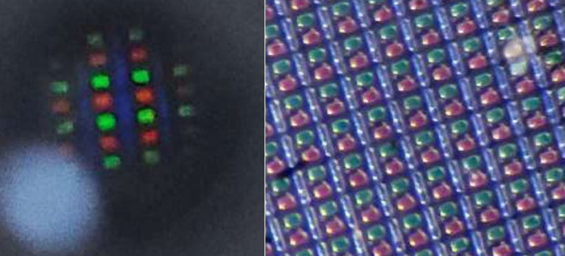
Main display: diamond-type RGBG (Pentile-like) arrangement for high PPI; green counted twice in area/aperture accounting; blue remains largest aperture among RGB.
Backplane & Drivers
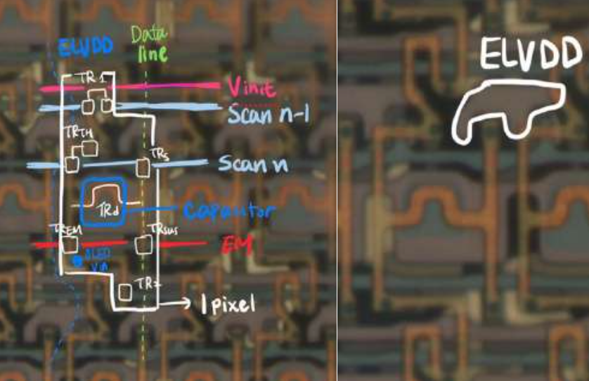
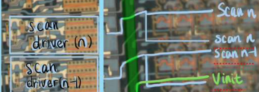
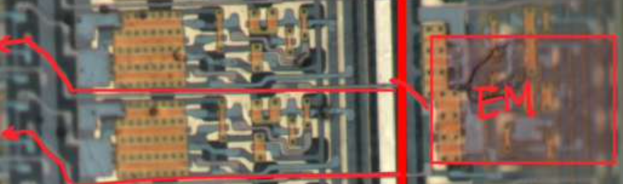
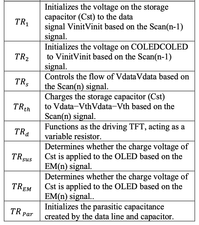
Symmetric Scan and EM drivers placed on both sides to shorten line length and reduce RC delay. Bottom side carries ELVDD, De-MUX and data lines. The cover display employs a 1:6 DeMux to reduce data lines; ESD protection taps into the data bus near DeMux. Sub-pixel is a 7T1C-type; per-TFT roles mapped from microscope images.

Measurements & PPI
Sub-pixel and capacitor dimensions extracted from microscope images (cover/main). Using backplane geometry, the device PPI was estimated at ≈ 431 ppi.
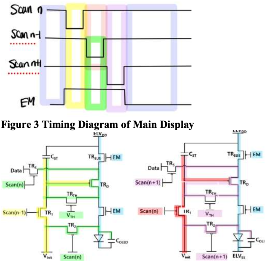
Timing Diagrams
Cover/main timing traced from driver outputs and EM coupling to adjacent pixel rows (n, n+1); diagrams reflect EM/scan sequencing consistent with symmetric driver placement.
 im
im
Discussion — Signal Integrity & Layout
(1) Symmetric Scan/EM drivers halve line length → lower RC delay and brightness drop along rows.
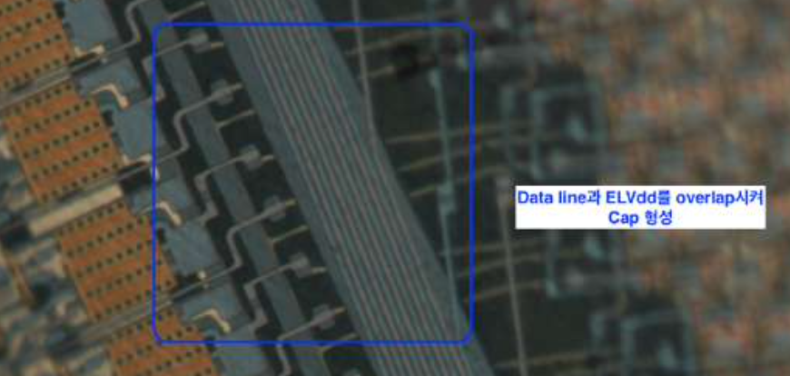
(2) Intentional capacitors between data and ELVDD assist delay compensation and tau matching.
(3) Staggered data-line routing near edges/punch-hole reduces distortion and supports higher PPI.
Punch-Hole & Hinge Region
Around the camera punch hole, lines are rerouted/stepped; certain EM/Scan/ELVDD segments are interrupted for stability. Hinge-area backplane shows no dramatic geometry change in this early Z Flip generation; later models likely refine stack/mechanics.
LTPS in Foldables — Reliability Notes
Poly-Si TFTs can suffer from strain-induced trap states at grain boundaries (mobility/Vth shifts) under bending. Mitigations include improved gate-insulator processes, curved-type active-layer designs, and aligning TFTs with the neutral plane to minimize mechanical stress.
Project Summary (Short)
Reverse-engineered Z Flip displays: quantified sub-pixel/aperture and PPI, mapped 7T1C backplane and symmetric drivers with 1:6 DeMux, confirmed on-cell touch (Y-OCTA) and TFE, and discussed routing/encapsulation choices and foldable reliability.